| 来源:N/A 更新日期:2008-12-15 15:13:38 阅读次数:7204 |
|
VIRTEX-5产品家族中的第一代产品用于高性能IO处理
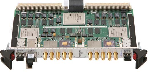
Latest: FPGA Technology, DDR3 SDRAM, and Advanced Interconnect Delivers 2 Gsps and Beyond Chelmsford, Chelmsford, Chelmsford, MA - June 26, 2008 - TEK Microsystems, Inc., the leading supplier of VXS-based digitizers has announced the Neptune-V5 6U VITA 41-compliant dual channel high-speed digitizer board. Designed to meet the needs of demanding sensor-processing applications across a range of environments, the Neptune-V5 employs three Virtex? 5 processors, advanced DDR3 SDRAM, and the latest communications technologies available. Full ruggedization has been designed into the architecture providing full support for harsh environments.
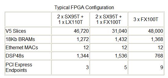
"The QuiXilica architecture is based on careful selection of the right features in the right places to solve the problem, as opposed to "checking the box" and using power, space and gates for capabilities that dont move the solution forward" comments TEK Microsystems, Inc. president and CTO Andrew Reddig. "Our architecture is designed to match the demands of streaming sensor I/O processing requirements. The Neptune-V5 integrates well into network and fabric centric systems, but we dont impose the overhead of a switched fabric all the way back to the front end sensor processing nodes. Instead, we use straightforward data flow mechanisms with the highest possible performance where speed is critical, and then add network oriented endpoint IP at the point that scalability adds value." * Virtex-5 LXT Platform - Optimized for high-performance logic with low-power serial connectivity * Virtex-5 FXT Platform - Optimized for embedded processing and memory-intensive applications with highest-speed serial connectivity
The FPGA can access two banks of DDR3 SDRAM of 512 MB each (1 GB total per FPGA). The DDR3 SDRAM uses 17% less power than DDR2. Memory and FPGAs are interconnected using multiple high bandwidth parallel and high-speed serial interconnections; thus data can be available within the processing chain as needed to meet a wide range of application requirements. Two e2v AT84AS008 10-bit Analog to Digital Converters (ADCs) are provided on the Neptune-V5, each capable of operating at sampling rates of 2.2 Gsps. Control functions on each ADC, such as sampling point adjustment, gain adjustment, and input DC bias adjustment can be accessed from the FPGA, through a two-wire, I2C-compatible interface. Trigger firmware can be implemented in the FPGA to fully synchronize data captures between multiple ADC channels on the same board or across multiple Neptune-V5 boards if required. Inter-board and system communication requirements are met using either backplane connections or multiple front-panel high speed serial Quad Small Form-Factor Pluggable (QSFP) and Small Form-Factor Pluggable (SFP+) modules which provide eight and six high speed serial links respectively operating at up to 6.5 Gb/s. Utilizing the embedded communication functions, as well as TekmicroS QuiXilica core and software library support (QuiXtream), the QuiXilica V5 Family supports the latest generation of Open Standard I/O protocols such as Gigabit Ethernet, Serial FPDP (ANSI VITA 17.1 & 17.2), PCI Express, Xilinx Aurora and Fibre Channel. Neptune-V5 boards operate effectively in laboratory, rugged air-cooled, and rugged conduction-cooled environments to meet the needs of deployed applications.
About TEK Microsystems, Inc. Founded in 1981 and headquartered in Chelmsford, Massachusetts, TEK Microsystems, Inc., designs, manufactures and markets a wide range of advanced high-performance boards and systems for embedded real-time data acquisition, data conversion, storage and recording. The Company provides both commercial and rugged grade products which are used in real-time systems designed for applications such as reconnaissance, electronic warfare, signals intelligence, mine detection, medical imaging, radar, sonar, semiconductor inspection and seismic research. For additional information see www.tekmicro.com. |